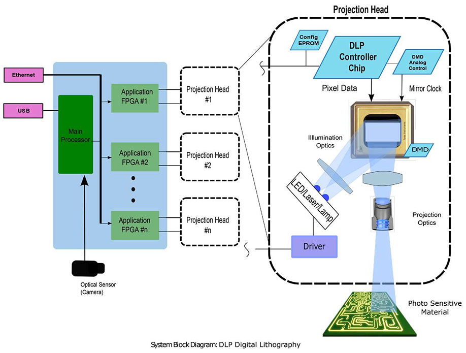
Digital exposure
Direct imaging digital exposure can be used to produce printed circuit boards (PCBs), ball grid arrays (BGAs), chip size packages (CSPs), flat panel displays, real-time barcode marking, and computer direct stencil printing – a printing process that directly sends a digital image from a computer to a printed board.
Compared to traditional digital exposure technology, direct imaging digital exposure has many advantages, including higher material flexibility, lower cost, and faster printing speed.
DLP ® High speed digital micromirror devices (DMD) provide a powerful tool for direct imaging digital exposure developers who require precision to reach the micron level, enabling rapid exposure in mass production situations, as well as lower operating costs.
By using DLP technology with programmable light control, developers can directly expose graphics onto photoresist film without contacting the mask. This reduces material costs, improves productivity, and enables rapid changes in graphics, making this technology very suitable for situations where the minimum overall size requires two exposures.
TI’s highly flexible chipset architecture also provides multiple system control and connectivity options, such as triggers for motor synchronization, sensors, and other peripherals.
