The FLXKU5PA development board is a mid-to-high-end FPGA development board built around the AMD/Xilinx Kintex® UltraScale+™ XCKU5P-FFVB676 core. It serves as a high-performance hardware platform targeted at high-speed data processing and communication system development.The board integrates on-board auxiliary components including power modules of various specifications,level-shifting integrated circuits, and high-precision clock management chips, fully satisfying the demands of diverse application scenarios such as high-speed signal transmission, data processing, prototype verification, as well as teaching and scientific research.
| Model | FLXKU5PA |
| MCU | Xilinx Kintex® UltraScale+™ XCKU5P-FFVB676 |
| Size | 95mm*170mm |
| Core Resources | 474,600 logic cells, 1,824 DSP48E2 processing slices, approximately 42 Mb RAM |
| Clock | 4 CMTs (Clock Management Units) |
| High-Speed Transmission | 16-channel GTY Transceiver 32.75 Gb/s |
| Category | Name | Specifications/Parameters |
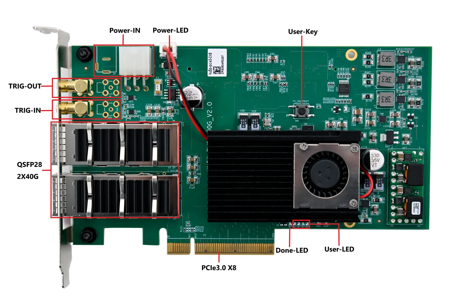
| Communication & Networking | PCIe 3.0 x8 | 1 |
| QSFP28 Optical Module | 2 x 40G | |
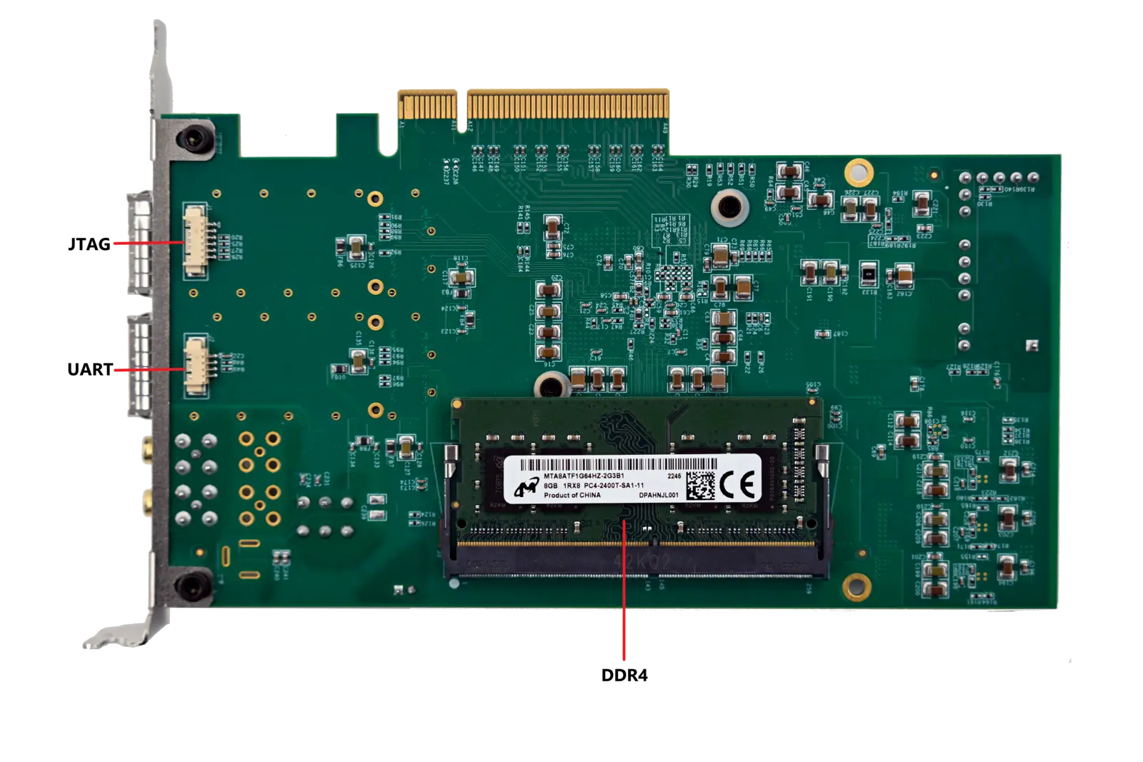
| DDR4 Memory | 1 16GB micron | |
| UART Interface | 1 | |
| SMA Interface | 4 | |
| Functional Peripherals | LED | 1 x 12V power-LED, 1 x normal power-on-LED, 1 x configuration complete-LED, 4 x USER-LED |
| KEY | 1 | |
| DIP Switch (8-position) | 1 | |
| Debugging Interface | JTAG | YES |
- Deployment in High-End Industrial Control Scenarios
- Development of 40G High-Speed Optical Communication Systems
- Factory Automation
- FPGA High-Speed Interface Protocol Verification
- Frontier Hardware Experiment Teaching in Higher Education Institutions
- IoT Device Development
- Board Management Controller
- Research Project Validation
- Hyperscale Storage