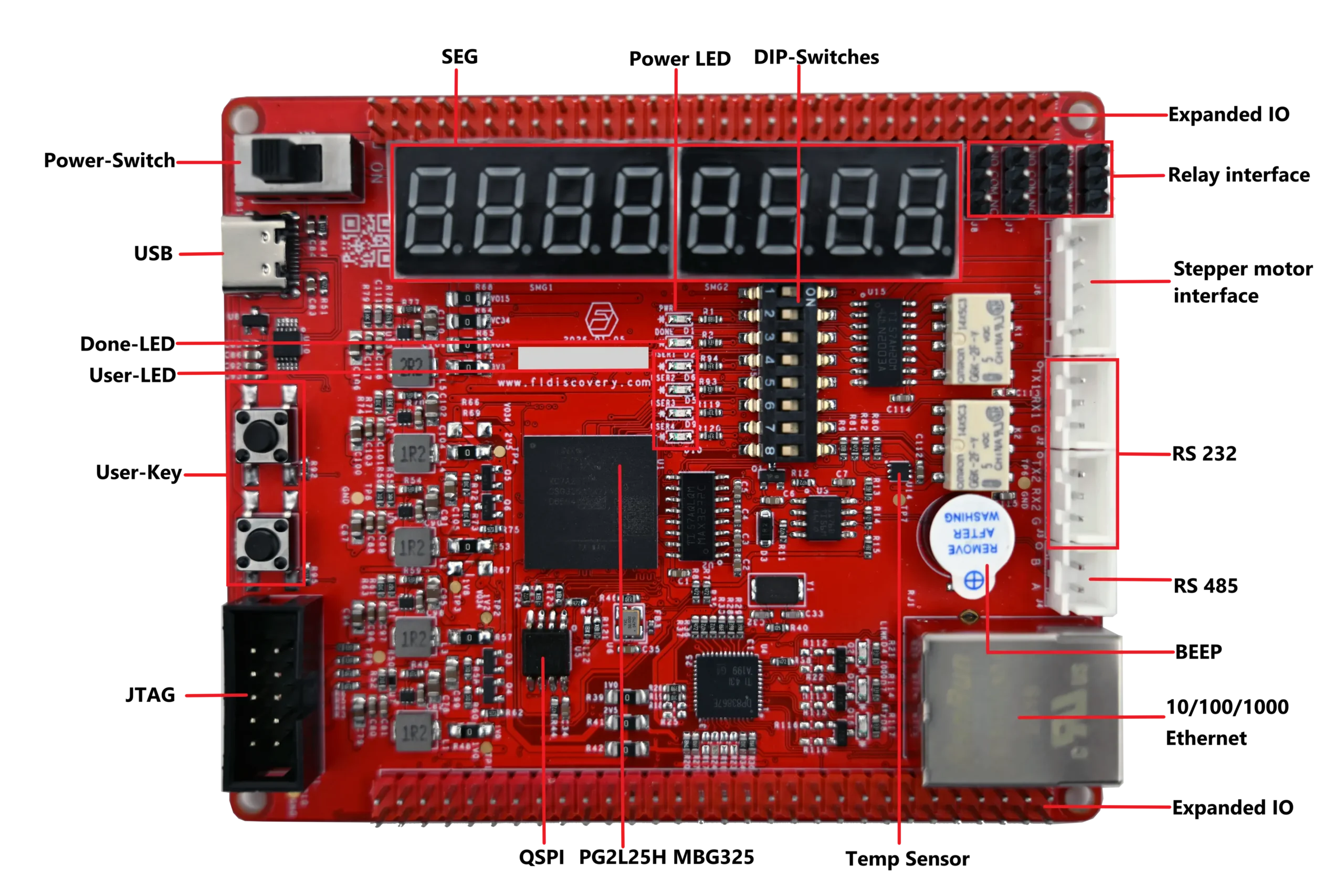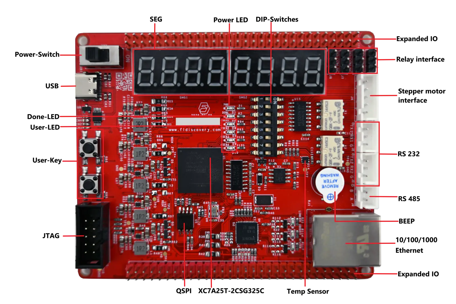
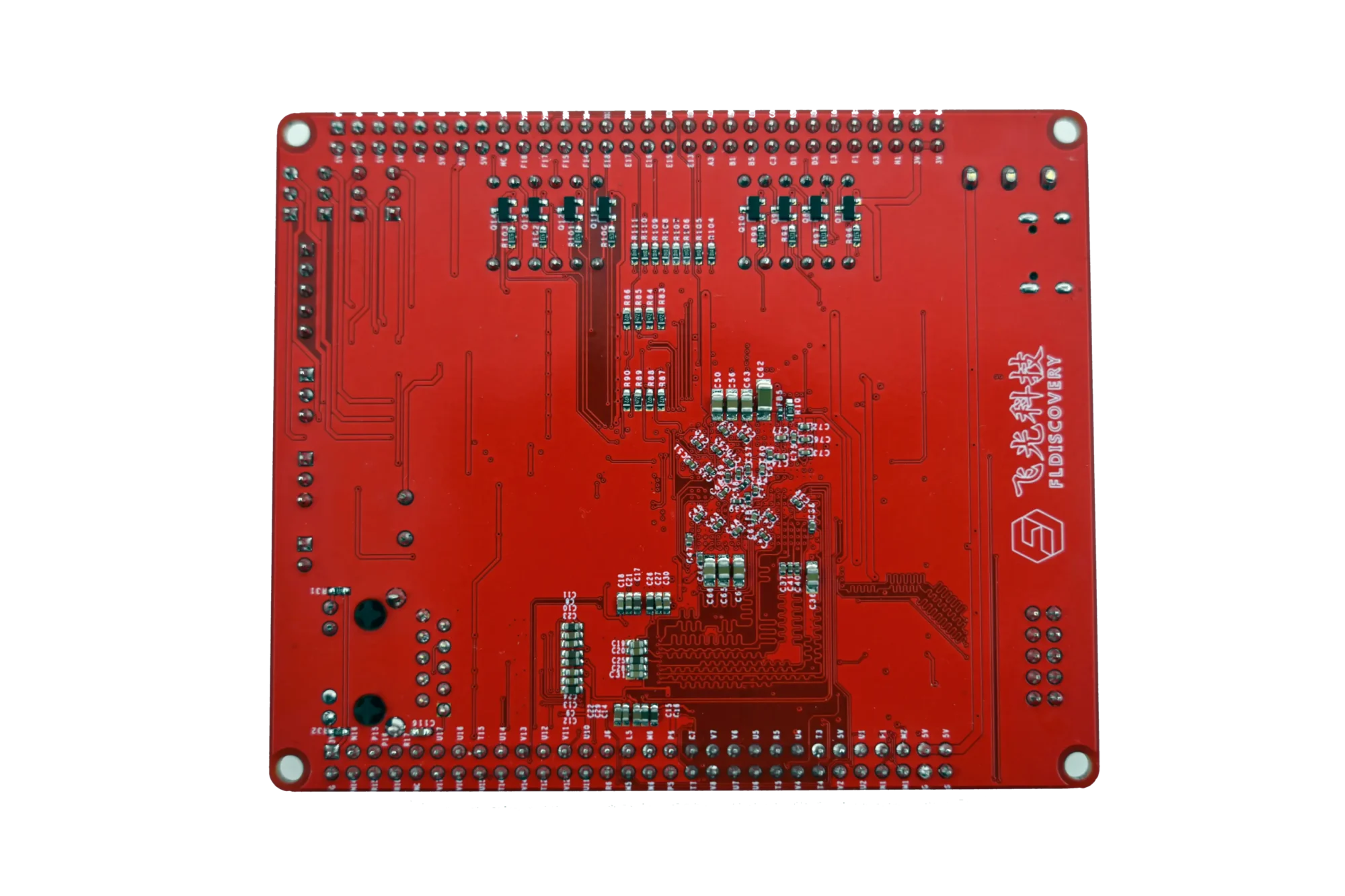
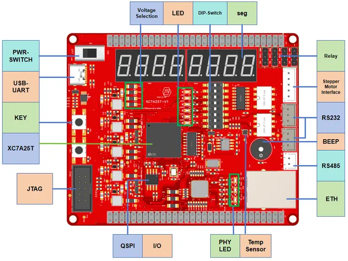
FLX7A25TA is a cost-effective FPGA development board centered around the Xilinx Artix-7 series XC7A25T-2CSG325C. Designed for industrial applications, prototype validation, and educational research, it combines comprehensive hardware configuration, robust expandability, and a convenient development experience. This makes it an ideal platform for FPGA beginners seeking to advance their skills and for implementing projects.
| Model | FLX7A25TA |
| MCU | Xilinx Artix-7 Series XC7A25T-2CSG325C FPGA |
| Size | 100mm*83mm |
| Core Resources | 23,360 logic cells, 80 DSP48E1 processing slices, integrated 45 36Kb Block RAM memory resources |
| Clock | 3 CMTs (Clock Management Units) |
| High-Speed Transmission | 1 GTP Quad (4 serial high-speed transceivers) |
| Category | Name | Specifications/Parameters |
| Communication & Networking | 10/100/1000Ethernet Networking | 1 |
| RS232 | 2 | |
| RS485 | 1 | |
| USB to UART | 1 | |
| Functional Peripherals | Temperature Sensor | 1 |
| CA-SEG | 2 | |
| Relay | 2 | |
| Stepper Motor Interface | 1 | |
| Other | 1 BEEP、1 PWR-LED、1 DONE-LED、4 USER-LED、2 KEY、1 DIP Switch (8-position) | |
| Expansion Interface | Expanded I/O | 92(Contains 10 pairs of high-speed differential signal pairs) |
| Expanded Power | Reserve 3.3V and 5V power supply pins | |
| Debugging Interface | JTAG | CON2X5-2.54mm,online debugging and program flash |
- Industrial Control
- Smart Hardware Prototype Validation
- IoT Device Development
- University FPGA Instruction
- Research Project Validation