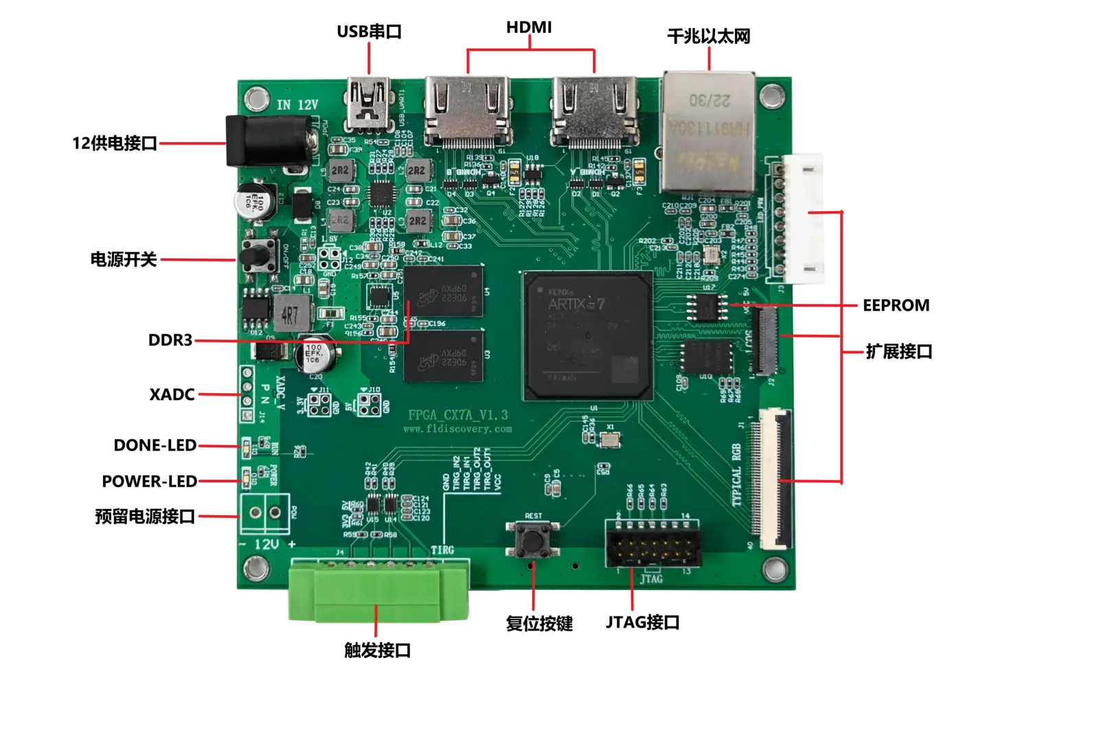
The FLX7A35TA development board takes the Xilinx Artix-7 Series XC7A35T-2FGG484C FPGA as its core control chip. It is a high-performance FPGA development platform with comprehensive functions and stable performance, and is well-suited for scenarios such as high-speed data processing and communication system development.
| Model | FLX7A35TA |
| MCU | Xilinx Artix-7 Series XC7A35T-2FGG484C FPGA |
| Size | 100mm*83mm |
| Core Resources | 33,280 logic cells, 90 DSP48E1 operation slices, and 50 integrated 36Kb Block RAM storage resources |
| Clock | Five CMTs (Clock Management Units), supporting frequency synthesis, frequency division/multiplication, and low-jitter clock generation. |
| High-Speed Transmission | 1 group of GTP Quad (4 serial high-speed transceivers), with line rate up to 6.6Gb/s |
| BANK Configuration | 5 HR BANKs (BANK14/15/16/34/35), supporting 1.2V – 3.3V multi-level and LVDS standards |
| Category | Name | Specifications/Parameters |
| Communication & Networking | 10/100/1000Ethernet Networking | 1 |
| HDMI | 2 | |
| IIC | 1 | |
| USB to UART | 1 | |
| SPI | 1 | |
| Functional Peripherals | SD Card | 1 |
| EEPROM | 2 | |
| DDR3 | 2 | |
| Stepper Motor Interface | 1 | |
| Other | 1 RST、1 PWR-LED、1 DONE-LED | |
| Expansion Interface | Expanded I/O | Including high-speed differential signals |
| Expanded Power | Reserve 12V power supply pins | |
| Debugging Interface | JTAG | Support online debugging and program flash |
- Industrial Control
- Smart Hardware Prototype Validation
- IoT Device Development
- University FPGA Instruction
- Research Project Validation